|
Homray Material Technology Co., Ltd
|

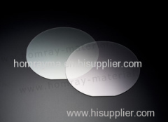
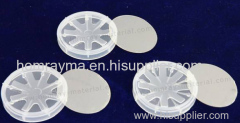
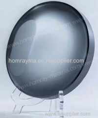
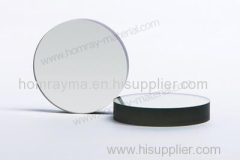
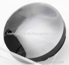
Test SiC wafer research Silicon Carbide wafer substrate
| Payment Terms: | T/T,WU |
| Place of Origin: | Jiangsu, China (Mainland) |
|
|
|
| Add to My Favorites | |
| HiSupplier Escrow |
Product Detail
Place of Origin: China (Mainland)
Brand Name: Homray Material Technology
Grade:Production Grade/Research Grade/Dummy Grade
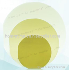
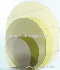
Type: 4H-N/6H-N 4/6H-
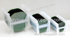
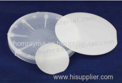
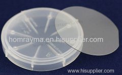
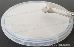
Homray Material Technology has developed SiC crystal growth technology and SiC wafer processing technology, established a production line to manufacturer SiC substrate of polytype 4H and 6H in different quality grades for researcher and industry manufacturers,Which is applied in GaN epitaxy device,power devices, high-temperature device and optoelectronic Devices.As a professional company invested by the leading manufacturers from the fields of advanced and high-tech material research and state institutes and China's Semiconductor Lab,we are devoted to continuously improve the quality of currently substates and develop large size substrates, as well as epitaxial technology.
The major products are 2 inch, 3 inch, 4 inch silicon carbide single crystal substrate, widely used in electronic devices with high power and high frequency, light emitting diode (LED) and other. light-emitting diode (LED) is the use of semiconductor electrons and holes in a combination of electronic components, is an energy-saving cold light source. SiC material has the advantages of low lattice mismatch with GaN, high thermal conductivity. The third generation of semiconductors represented by SiC has a high bandwidth, high thermal conductivity, high field breakdown, high saturation electron drift rate, stable chemical properties, high hardness, abrasion resistance, high bond.
Related Search
Find more related products in following catalogs on Hisupplier.com
Company Info
Homray Material Technology Co., Ltd [China (Mainland)]
Business Type:Manufacturer
City: Suzhou
Province/State: Jiangsu
Country/Region: China (Mainland)